The chip stands as the cornerstone of today’s digital age, impacting every aspect imaginable. Across nearly every societal process, this inconspicuous piece of technology plays a critical role: mobile phones, laptops, self-driving cars, the banking system, medical equipment, the internet, and even coffee machines all rely wholly or partially on chip technology. The development of chip technology, with the semiconductor as its fundamental element, has been the result of extensive research, experimentations and happenstances dating back to the 1950s. Dutch companies Philips and NXP Semiconductors have played pivotal roles in the advancement of the international semiconductor industry.
On October 26, 1953, Philips began assembling semiconductors on a modest scale in the Twentsche Bank building on Mariënburg in the center of Nijmegen. At that time, Nijmegen was primarily a residential area with a small-scale tourist center, but it rapidly industrialized following the Second World War. Over the subsequent decades, Philips’ operations in Nijmegen expanded from three to over fifty-five buildings, and its workforce grew from 50 employees in 1953 to more than 5,000 by the turn of the century. Within Philips, various Main Industry Groups (HIGs) were established. The chip factory in Nijmegen was initially part of HIG Icoma (1952-1965), later becoming part of Elcoma (Electrical Components and Materials, 1965-1988), which manufactured various electronic components. The Elcoma name was solely used in the Netherlands; international branches adopted local names, such as Valvo in Germany, Faselec in Switzerland, RTC in France, Signetics in the USA, MBLE in Belgium, MINIWATT in Denmark, and Mullard House in the United Kingdom. In 1988, all brand names were consolidated under the name Philips Components, which subsequently split off in 1991 to form Philips Semiconductors due to the rapid growth of the semiconductor business. On October 1, 2006, Philips Semiconductors became an independent company separate from Philips, operating under the name NXP. Until 2010, Philips retained approximately 20% of NXP’s shares, with the remaining shares held by private equity investors. Today, NXP is an independent company listed on the US NASDAQ-100 stock exchange. Meanwhile, Nijmegen has become renowned for its chip industry, leading to the establishment of numerous semiconductor companies, most of which are located on the Novio Tech Campus, the site where semiconductor activity in Nijmegen originated.
In 2023, the archive of Philips/NXP’s cultural technology heritage was transferred to the LINK foundation. This collection provides an overview of the evolution of microchips and related technologies originating from the semiconductor industry in Nijmegen. Established in 2021, the LINK foundation emerged from a unique collaboration between NXP Semiconductors and the Department of Design Art Technology at ArtEZ in Arnhem. Its mission is to preserve and promote cultural-technological heritage, with a specific focus on the history of chip technology in the Netherlands. The exhibition Pluralities of Scale. 70 Years of Microchip History marks its first public event, bringing to life the past and present of the chip through archival documents, accounts from former Philips/NXP employees, and contemporary artworks. The exhibition explores the chip’s societal impact along four thematic lines, revealing both its opportunities and dangers, and how this technology has permeated every facet of society: from geopolitics and labor structures to art aesthetics. In discussions with the initiators, Martijn van Boven (MvB) and Florian van Zandwijk (FvZ), we delve into the impact of NXP Semiconductors and the significance of its archive in reshaping our understanding of digital society today and the broader implications of technological development.
Annet Dekker (AD): How did you get involved with NXP semiconductors?
Martijn van Boven (MvB): At the time, I was still the head of the at the Design and Art Technology Department in Artez, Arnhem. So, about five years ago, I received an email from NXP semiconductors, asking, hello, we’re NXP semiconductors, we have an archive, and we don’t know what to do with it, but we would like to create more access and visibility to it. As our assistant of the department Anke mentioned, this was the email we’ve always been waiting for. They had just used a simple Google search for “art and technology” and then we were one of the top hits, so in a sense it was pure luck.
I went to Nijmegen. NXP has a huge manufacturing plant consisting of different buildings: a main manufacturing plant where they produce the chips themselves, including the offices and research buildings, and then there are many old buildings where they used to produce other earlier versions of wafers etcetera. In one of the empty buildings was their archive. The place was pretty run down, there were mainly boxes filled with stuff: lots of paper but also all kinds of objects, drawings and elements of prototypes. Literally in the corner, they had the print that’s now the main part in the exhibition. Rolled up catching dust. When I asked them to see it, I was baffled. Stretched out in front of me was a drawing of about 5 meters long and 1,5 meters wide. Yet, it only showed a small part of a chip for a 100 Hz television.
I have a good sense of the history of computer technology, but I had never seen how these things were made: now I saw this drawing that included detailed plotter parts, handwritten notes, but also stains of pens and coffee. Also many of the other things I had never seen or really knew about. In a way the experience was a bit unsettling: it shifted my perspective of how technology was made through this visual aesthetics language of graphs, drawings and plans.
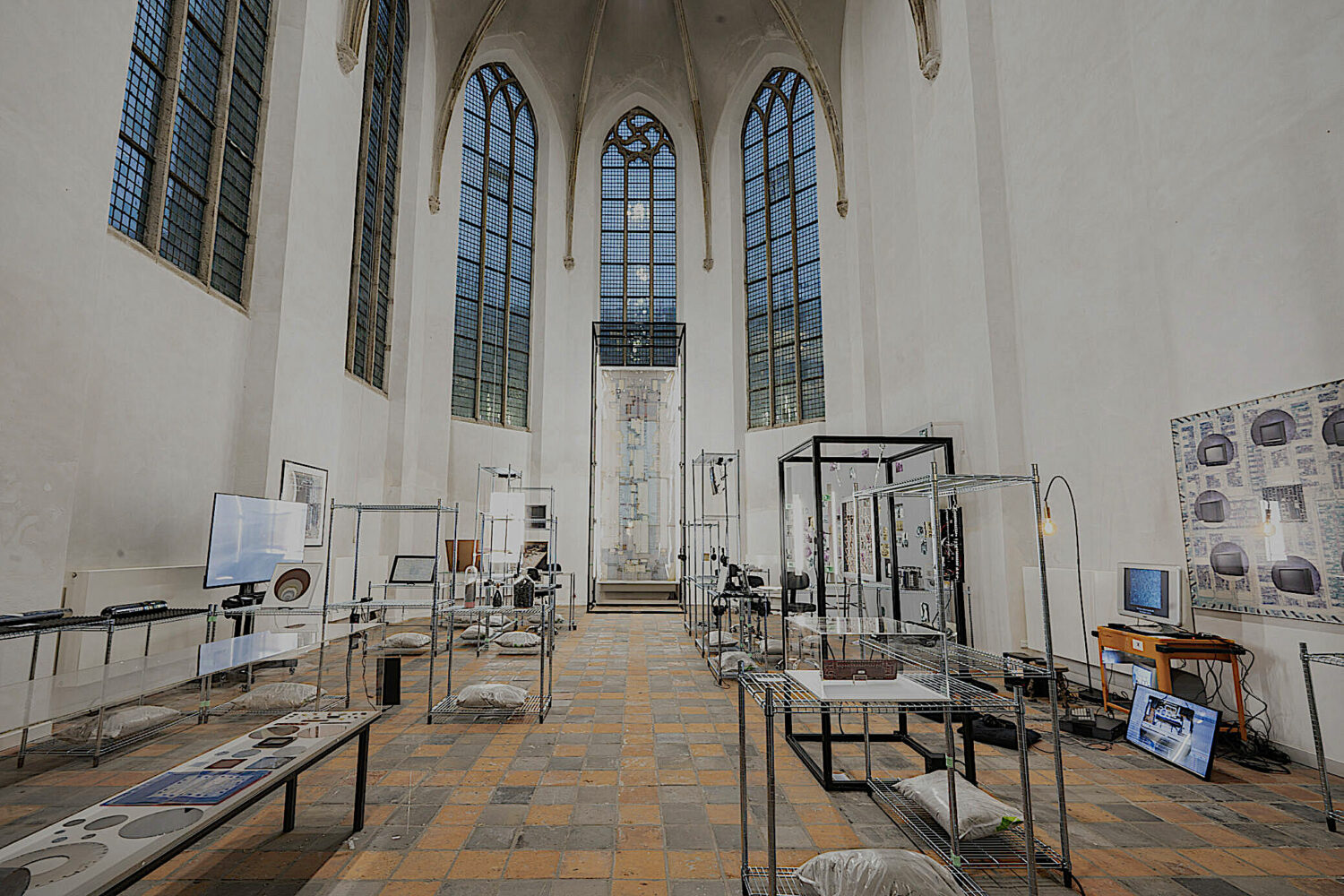
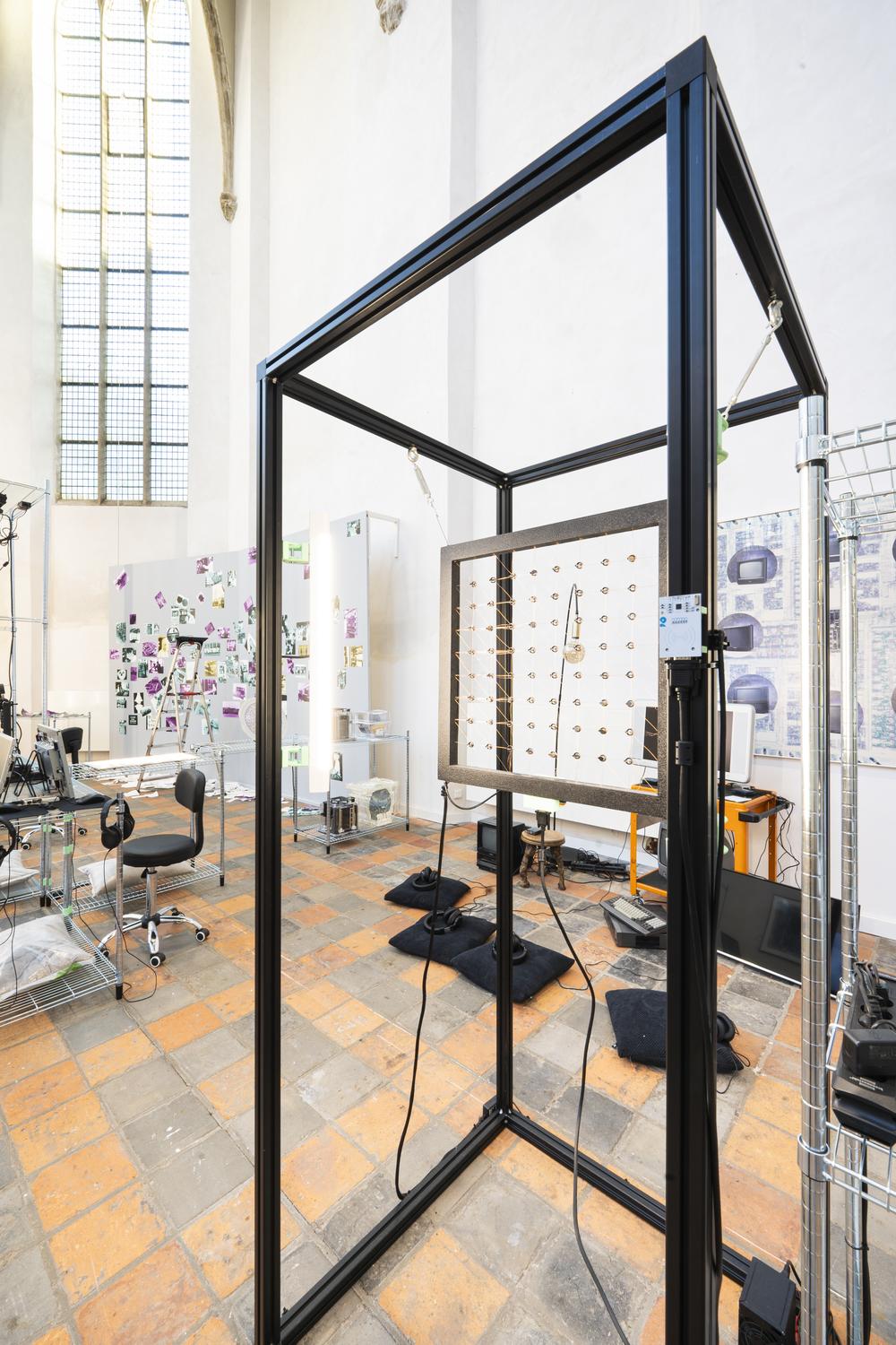
Pluralities of Scale. 70 Years of Microchip History, Nijmegen’s House of History, Nijmegen, January 2024. Photo: Eva van Boxtel
AD: Can you describe the historical relevance of NXP?
MvB: Philips was one of the few electronic manufacturing companies that did everything in-house. They had their physics lab called the Natlab where they would do fundamental research from which they created applications, that turned into consumer products. So, the beauty and relevance of NXP was their continuous line from fundamental research to consumer products. At the same time, they employed 250,000 people in the Netherlands. So Philips had a strong impact on technical development in the Netherlands, but they were also one of the first to develop and manufacture microchips on an international scale which influenced other big tech companies like Samsung in Korea.
For us, the current relevance is the availability of the archive that still has all the early records, the drawings, as well as many prototypes and artifacts. And many of the former employees are still around and able to tell the stories of how they developed the chips. So, the socio-technical fundaments of the contemporary digital era are still available to trace. This kind of knowledge is often taken for granted, but for most inventions we don’t have any sources to go back to that really explain the early days of experimentations and development.
Through the interviews we did with the former employees we learned that most worked their way up in the factory. For instance, some came from poor working-class families, who wouldn’t go to a university, and instead started working for Philips who would provide for their education. Such a person later came up with the invention of the electronic scheme for color television. Philips was based in Eindhoven and Nijmegen, both at the time poor areas in Netherlands, they provided work, education and they also build housing for their employees, which is still clearly visible in Eindhoven (STRP areas). So, there is also an important ideology behind NXP and Philips as a company. A multinational like Philips can be compared to current technological companies like Amazon or Facebook, but it has a completely different social base which derived from Marxism – Karl Marx is said to have been a friend of the family. Next to providing this broad learning environment, in the Netherlands it was the first company to start pension schemes for their employees. I believe it is important to stress this social fundament, as it shows how things can be done differently. So, the archive doesn’t only show the fundament of the digital era, but it also has many stories to tell about how companies influenced social structures.
AD: Do you believe that this ideology is also mirrored in the development of the chips themselves? Could it be that one of the factors contributing to Philips’ success lies in how they structured their processes—both in terms of manufacturing and their underlying social foundations?
MvB: This was always one of my questions to the former employees, but the reply was always no. They had an interest in engineering and were interested in tinkering with radios, and the culture of collaborative working around it. Hence for them micro-electronics was an obvious path to choose. But I never heard them say, yeah, I really felt that I was part of something new. It was just a job. They didn’t see it as world changing, or being at the brink of a new era of computation. I think this partly is due to the abstraction of the work. They would work with something they had never seen before, there were no applications, methods or set guidelines to follow. It was mostly functions on a piece of paper, drawing lines and calculating voltage dividers, etcetera. There was nothing fundamental about it yet: it was experimentation and seeing where things could line up or lead to, but not necessarily knowing what that would be exactly.
Florian van Zandwijk (FvZ): Also, Philips was also not selling it like the next new thing. This notion of groundbreaking developments and ‘laying the foundations of microchips’ came only in hindsight.
MvB: Indeed, and this is also what fascinated me: none of these people were talking about their work as being at the frontiers – the pioneers of the digital cultural transformation. They never thought like that.
AD: The technology we currently use is significantly more abstracted; indeed, the human aspect of its manufacture is often overlooked. Behind the sleek interfaces, all the intricate processes remain largely invisible, with the true labor often hidden away in sweatshops. However, from your research and the exhibition, what truly emerges is the collaborative essence of the work and the profound impact of human involvement. This is also evident in the progression depicted in the photos you have found and selected: it begins with a highly social culture, bustling with numerous individuals, and gradually evolves into a more technologically-driven environment, resembling a laboratory setting.
FvZ: The archive of NXP semiconductors spans a period of several decades, from 1950 to 2000, and we found many photos from that whole era. These photos tell a visual story of the company as well as of the development of labour in the Netherlands: indeed, spanning from the manual work performed by women to automated processes under the supervision of men, and how workers hidden in protective clothing were replaced by machines. We asked Alina Lupu to make sense of the collection and she decided to mark the photos in different colours and give people the opportunity to create their own visual narratives. So, we build a wall for people to attach the images, to replace or to remove others and hence there is a lot of room for interpretation and speculation.
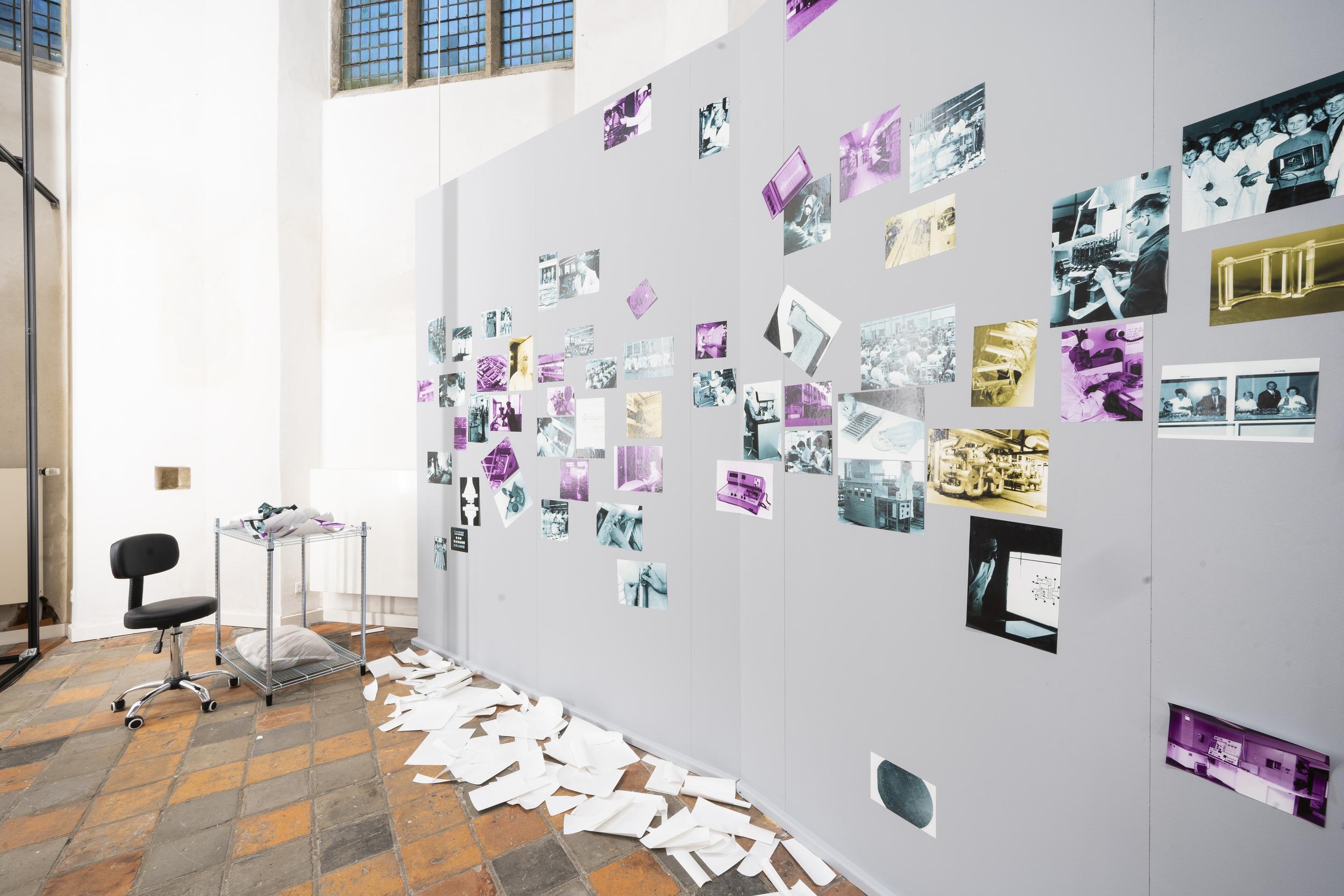
Alina Lupu, People Behind Machines, 2023.
MvB: Essentially the fundaments of the technology are still the same, but indeed the process is much more abstracted. The way we use technology now is completely different from what it was. You could open up your TV and see what’s inside, which is near impossible now. With the exhibition, we also wanted to show that technology starts with human doing things, and often doing it together. The rows and rows of these classic photo books that we found in the archives showed the employee parties, company lotteries, and other social gatherings. Also the people we interviewed kept coming back to the importance of the social fabric of their work: they were in it together.
FvZ: Philips also framed that in a way by providing a specific context. They all worked on the same work floor. They would be in the same sports clubs. They would go to the same doctor. They were all part of this feeling that they were part of a bigger thing. So this also meant that no one would claim to be this one person that knew it all or that did it better. A very socialist structure.
MvB: And these social structures were also necessary. Indeed, anyone could come up with an idea and it would be tested. That was the company’s culture. Nowadays this is often used as a marketing trick.
AD: Was the intertwining of the social and the work something you aimed to convey with the title The Pluralities of Scale?
MvB: The title works in different ways. On the one hand it shows the continuous shifts between small and large: the micro-chip is something tiny, but it is used in numerous appliances, which affect us on an individual scale, as well as on a societal or planetary scale, and even outside of our planetary scale. Essentially, as Ari, one of the interviewees mentioned, it doesn’t matter the same chips are used in Russian rockets and coffee machines. At the same time, the manufacturing process of chips is massive: it goes from the rough and unhealthy mining labour, to the extreme precision and delicacy that is needed in order to produce a semiconductor which is done in very clean environments in which the wafer needs to be extremely flat and all the atoms need to align. The contrast of all these processes of manufacture is intriguing. Basically, everything we found in the archive could be scaled up or down at the same time. For now, we believe it is important to develop a language around the fundaments of these technologies. It is about introducing a visual language that is completely unknown to us, the general public, and to make it part of our daily consciousness, or at least to understand how these things developed and are manufactured.
FvZ: So, on the other hand, in the exhibition we decided to focus on four scales: technical, visual, social and global.
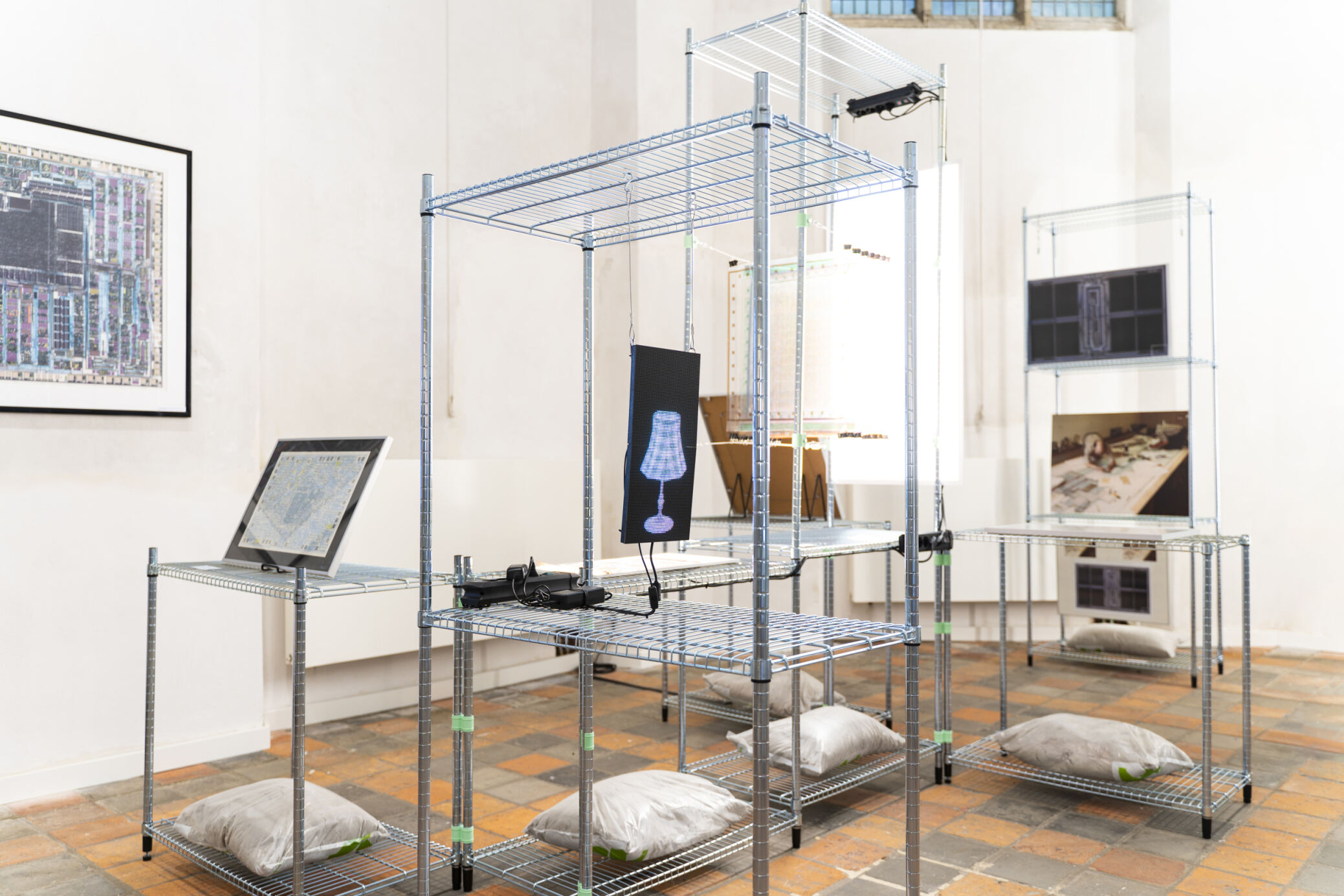
The technical scale introduces the way chips are produced and where they come from, hence we used a bag of sand at the beginning of the exhibition which is both a statement but also where it begins and from there, we show the silicium bar and how that is cut and polished into discs that are then printed on, etcetera. We also found large glasses filled with diodes and transistors. However, the technical scale is only a simplified version of the whole process.
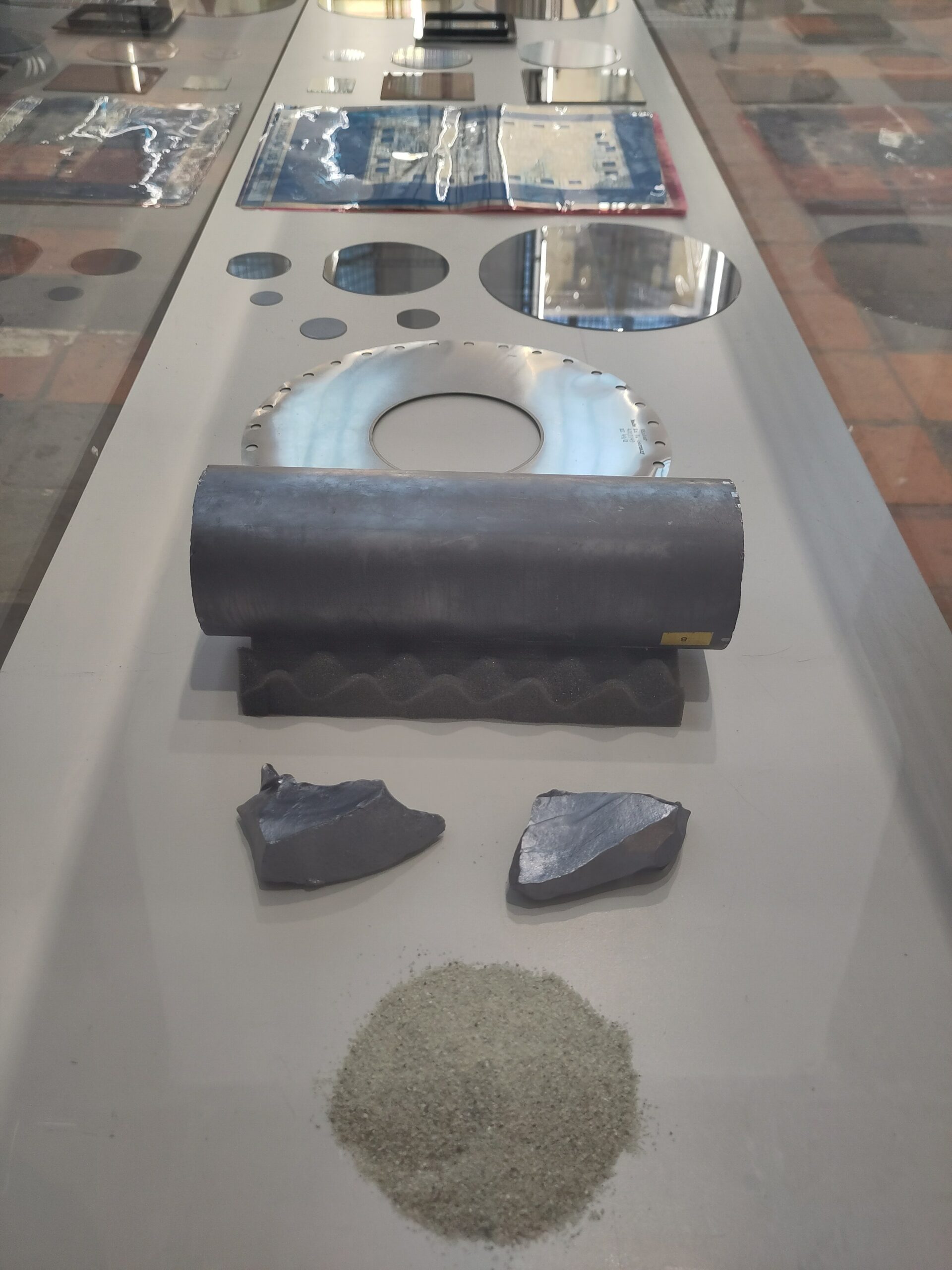
From sand to wafer – some of the materials used to make microchips, Pluralities of Scale. 70 Years of Microchip History, Nijmegen’s House of History, Nijmegen, January 2024
From the technical physical stuff, or physics, we move into the design process. This is the more engineering point of view and to which it is easier to relate to because there is a visual appealing aesthetics that we understand and perhaps relate to modern 20th-century art. It shows all kinds of prints and the layouts that were made before the chip is actually being built. For instance, we found series of transparent sheet in which each sheet shows a specific layer of the chip design. Still form follows function, it’s all about efficiency. For instance, the different colours show you which layer it is. The placement is important, because it has to fit in as small a scale as possible. And then it turns out to be something visually intriguing, which they don’t really noticed. Yet at the same time, we found several framed drawings – even of things that were mistakes. But the centerpiece is the hand-drawn construction of a part of the ‘Octopus’ chip for a 100 Hz television from 1968. This small element is already 488 x 168 cm. In the 1960s, the early days of the chip, all chips were designed by hand. At a certain point, the main lay-out was plotted but then all the elements were drawn by hand.
MvB: The drawing is such an important part of history: both technically, socially and aesthetically – it should be in the collection of the Rijksmuseum!
What it shows is that humans are behind the high-technology world that we are living in. The drawing is filled with coffee stains, and as we learned from Harrie Veendrick who co-designed this, these were from his colleague who was a real coffee addict, drinking up to 12 cups a day – which you can see on a photo we found in which the two of them crouching on the table, on the drawing, putting the elements in place, inserting short notes, etcetera. It exemplifies so clearly the importance of the graphic crafts of lithography and masking and how these are all part of these early processes, while it also brings out the human stories.
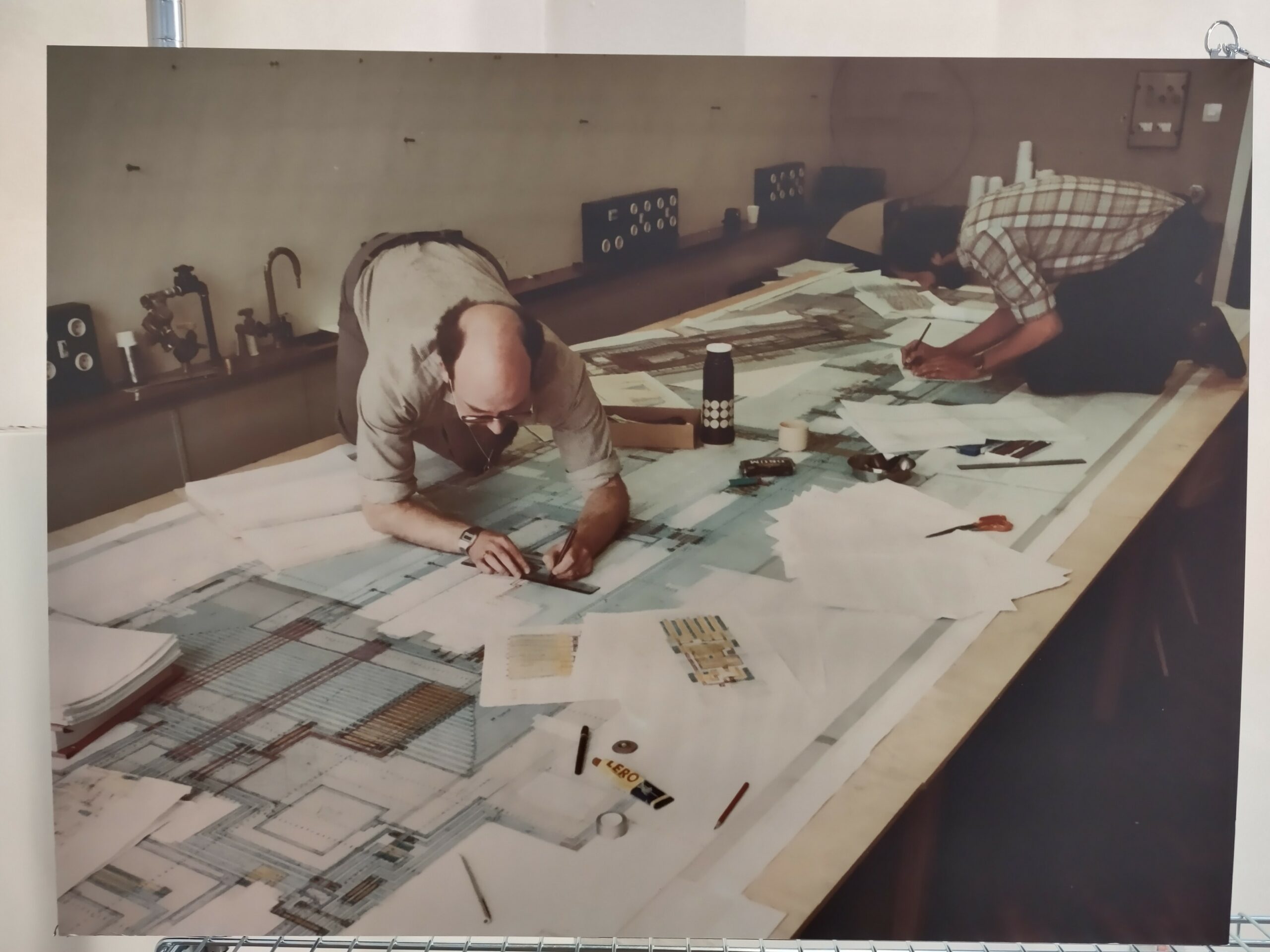
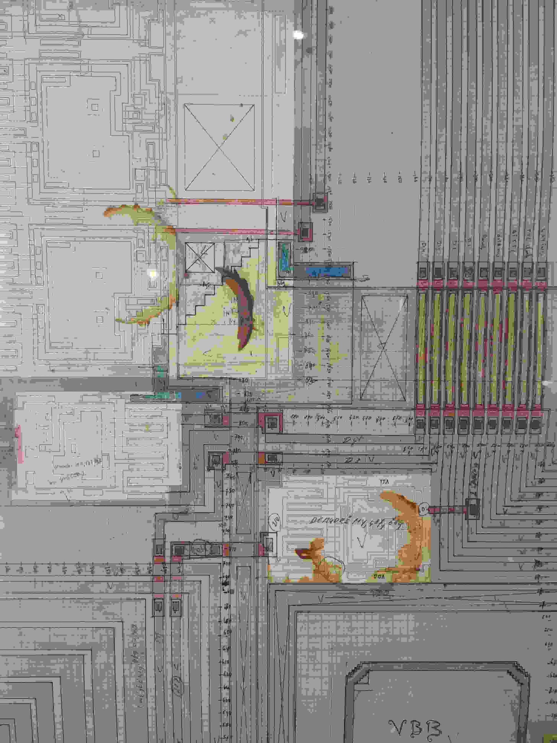
Octoplus microchip 1982, a small detail of the 488 x 168 cm (1/8 of the full scale) construction drawing depicting a segment of a 100 Hz television ‘Octoplus’ microchip from 1982 (R), made by Harry Veendrick and Leo Pfennings (L). Pluralities of Scale, 2024
FvZ: Which indeed brings us to the social scale, which presents the production environment and the coming together of people: as we just mentioned, lots of photos of people laughing, of women working together. It provides an alternative picture of how the future is being made: sourced through local production and in collaborative working environments.
The last scale is to show the global use of chips in various applications: the artifacts. In the end the focus and selection of these four scales also followed from what we found in the archive, but there are many other levels you can address.
AD: In numerous exhibitions featuring machinery from the past, there is often an overpowering sense of nostalgia. However, you adeptly navigated a path that veers away from pure nostalgia without outright rejecting its influence.
FvZ: Yes nostalgia may play a role, but we wanted to present the exhibition as a starting point for further discussion. All the objects tell their own story and they can be connected in various ways. We noticed how this works really well in tours with different groups, particularly when it included people who were part of that era, they would recognize certain things or even people and new stories would develop. I don’t think this is necessary nostalgic but these are elements to trigger memories that can relate to wider issues that are still relevant today.
AD: Next to the objects and drawings you also present artworks, was that also a way to step away from becoming overly nostalgic?
MvB: Initially the artworks were part of the assignment for the students. They had to create a response to what they found in the archive.
FvZ: Yes, and we were very excited by what we found. But now a few years after, and also taking into account your point of nostalgia, I think the artworks also prevent an over-emphasis on nostalgia because they bring the old into the contemporary. It flips the objects in the exhibition to how we see this technology now. They also don’t fetishize the objects but they managed to move to some of the main intentions that was part of NXP.
For instance, the work by Benjamin Earl is a series of led screens showing lamps. It refers to a meme that was going around on Reddit which stated “Lamps in Video Games Use Real Electricity”, which was picked up to proof if turning on a lamp uses more electricity than keeping it off. Eventually, the answer was that it depends on the type of medium you use. Benjamin turned this a bit around, and played with the notion of images of lamps on screens becoming lamps. It relates both to the difficulty of how to visualize light in a video games, and how we use the materiality of screens. So, essentially this has little to do with the NXP archive, but it has everything to do with the fundamentals of what NXP does. It shows the paradoxical relationship of what you see on the screen: what it means on the inside (the lamp as technical material) and from the outside how you experience it (the lamp as light). So, it is more a philosophical take on what it means to talk about digital or physical, and if there’s even a difference in those things.
Benjamin Earl, Lamps in Video Games Use Real Electricity, 2023. Photo: Eva van Boxtel
AD: What were some of the unexpected surprises or insights you gained throughout this project?
MvB: I’ve been working with computer technology my whole academic life. First, I primarily used them as tools, when moving into Sonology they became media to explore and experiment with, to create all these new sounds. Now, talking with these former NXP employees, made me realize the importance of the human element in all the technology we use. The notion that these people, they made the technology -and the world- that we are living in right now. But they never thought about the idea of digital culture, or the 21st century, these were just people living in small towns in the Netherlands. And many of the things they developed happened due to the limitations they had to deal with. For instance, with the large drawing of the ‘Octopus’ chip they had to deal with limitations of the size of the printing machine as well as the memory of the computer that was printing the layout for this drawing. So, if something needed to be printed, a truck was sent from Nijmegen to Eindhoven, and back again. And if they made a mistake, the truck with all the papers had to return. It really revealed to me the cumbersome way of working that we can’t imagine anymore, but also that we never think about technical development in this way. I believe there is a huge misconception with many people –which included myself– about the idea on how the future is made. So, what this archive has showed me is that the future was made with men spilling coffee on technical drawings, and people discussing about who this woman was on this photo, and Harrie remembering misfortunes of his colleague.
I think the collective memory of how we think modern technology is made, is in need of revision. Things are done completely different than you can imagine. This also comes back in the video NXP – Through the microscopic glass by Michelle Feelders. She decided to focus on the men who have to watch the microscopic process and in particular their ideas about what they see when checking how these microscopic images are being made.
Michelle Feelders, NXP – Through the microscopic glass, 2020, video. Photo: Eva van Boxtel
So, every time when we would do a tour with the students through the manufacturing plant, we would be introduced to different stages of the production process. Most of the production process is actually about quality control, because your chips need to be completely 100% fail safe. In some cases, the only thing someone may do is look through an atom microscope to see if a wafer has any imperfections. The person we met also made a collection of screenshots which he inspects; looking for potential dust particles on top of the wafer. He analyzes the specs and starts to metamorphize them, like, look, this looks like a bike, and this looks like a house, perhaps this is a dog? Even though it is illegal to make these screenshot (as you don’t want your client to know that there are imperfections on the wafer) he was happily showing them to us; also because he knows that despite the particles the wafer will function fine. So, Michelle interviewed him and translated his abstract landscape into a video. We get immersed in his gray-scaled world, where the light doesn’t transmit. The video shows another side of technology: starting at the scale of a printed circuit board to then scale up to tiny dust particles that are given names. In that process you start to experience technology in a different way. The video becomes this microscopic world of electronics that we have never and probably never will see this way, whilst we deal with them on a daily basis. The increasing complexities of an unfamiliar world are made tangible through the imaginations of the people checking them. And where any mistake could potentially have catastrophic results, they show us the beauty of a surrealist world. Yet it is one that is completely controlled and monitored.
AD: What implications might this exhibition hold for our understanding of the future development of technology, and could it potentially influence our perception of the current technological landscape?
MvB: An important aspect for us is the demystification of how technology is constructed. When meeting with these former employees and hearing their understanding of the process opened up new perspectives. To them, the digital world doesn’t exist, there is no magical digital cloud: it is all about devices having some of their products inside, and they know how those products work.
FvZ: Yes, we wanted to get rid of the mainstream marketing narrative of a seamless digital world. These people talk about sand, how it goes into the machine that makes sausages and cuts it into salami slices. It is not mystifying the technology. In order to understand the contemporary world, we need a different narrative of the digital. The scales we present now are just scratching the surface. You could take one of them and create a new exhibition just about that one element.
MvB: In the first few years there was just an exchange between students and archive. Florian and I have been working on this particular project for about a year. There is so much more in the archive: there are many videos, and we found a compact disc with an explanation on how to open it and take it out, it says sample disc number three, but we haven’t yet opened it. It could simply be promotional material, but it could also be the third CD that was ever made.
There are so many stories to tell. The archive shows all the different scales and layers of chip production which perhaps makes this archive unique in the world. Also, through the talks we had with the engineers it became clear how they all have their specific ways of working, like a painter doing specific brush strokes, and the same can be seen in the work they did.
FvZ: A good example of the detail of this is also the work Monument for Memory by Bram de Groot. The project is a monument to the lost craftsmanship of one of the first methods of computer memory manufacturing: ferrite core memory assembly. Microchip development company NXP relied on passionate craftswomen to weave these core memories by hand. By closely studying the weaving techniques, Bram recreated a 64-bit memory and lets it interact with one of the smallest NXP memories to date, the NFC (Near Field Communication) chip.
Bram de Groot, Monument for Memory, 2019. A monument to the lost craftsmanship of one of the earliest methods of computer memory manufacturing: ferrite core memory assembly. Photo: Eva van Boxtel
MvB: If there is one thing that I learned from all these interviews is that there was no clear sort of idea in which direction this technology was heading. Everything was still very diffuse, there were no standards, many things happened haphazardly. People discovered things without a big plan, and without a genius mind: it happened through limitations, accidents and collaborative work. There was a mix of machine technology, human thinking and tinkering, mathematics, held together by limitations. This process now flipped around, the human hands and the limitations are replaced by more technology. In the factory people are now merely bringing a wafer from one side to the other, because there is a monitor that displays that number 12 needs to go to number 16, someone walks over and does it for maybe less than ten euros an hour. I think this archive tells both sides of the crossfade. Perhaps if standardization wasn’t pushed so much, we would have a way more diverse computational landscape. And that is something that I’m still very eager to figure out.
Bios
Martijn van Boven (https://www.474746.org/) studied Image and Sound at the Royal Academy of Art in The Hague. His work manifests itself in a variety of (digital) audio-visual media; installations, films, videos, performances and various collaborations with composers, in which he combines the possibilities of contemporary computer technology to generate abstract images and (ambient) sound environments. In 2003, he co-founded <>TAG a cross-media platform in The Hague. From 2008 to 2016, he was an editorial board member of the Sonic Acts festival, and from 2012 to 2021, he was also Head of Department of Design Art Technology and lecturer of Media Archeology at ArtEz Institute of the Arts in Arnhem.
Florian van Zandwijk (http://www.florianvanzandwijk.nl/) is an artist with a focus on the inseparable connection between human and technological sensorial perceptions in today’s digital age. His work takes shape in diverse forms and roles, encompassing everything from standalone art pieces to the design and development of various projects and formats in the cultural field. He uses simple gestures as well as visual essays to research present human and non-human Ways of Seeing. Through this exploration, Van Zandwijk aims to unravel and provide insight into contemporary themes related to the biases and limited capacities of human and technological perception. Van Zandwijk’s work touches on topics like artificial intelligence, work, social media, mass surveillance, and computer vision.
Annet Dekker is a curator and researcher (http://aaaan.net), currently serving as Associate Professor of Archival and Information Studies, and Comparative Cultural Analysis, at the University of Amsterdam. Additionally, she holds the position of Visiting Professor and co-director of the Centre for the Study of the Networked Image at London South Bank University. She regularly contributes to numerous collections and journals, and has edited several volumes, including Curating Digital Art: From Presenting and Collecting Digital Art to Networked Co-Curating (Valiz 2021).